HSC Resources · Physics 2
Ch10 Semiconductor and Electronics
Lecture slides and notes for Ch10 Semiconductor and Electronics from the Physics 2 module in HSC Resources by Md Ahbab. 14 pages.
Content Preview
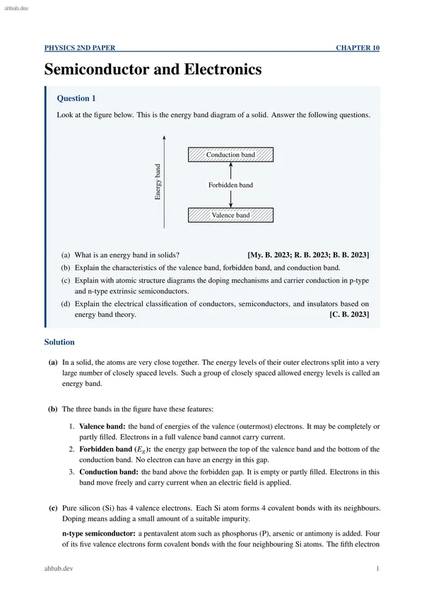
PHYSICS 2ND PAPER CHAPTER 10 Semiconductor and Electronics Question 1 Look at the figure below. This is the energy band diagram of a solid. Answer the following questions. Energy band Conduction band Valence band Forbidden band (a) What is an energy band in solids? [My. B. 2023; R. B. 2023; B. B. 2023] (b) Explain the characteristics of the valence band, forbidden band, and conduction band. (c) Explain with atomic structure diagrams the doping mechanisms and carrier conduction in p-type and n-type extrinsic semiconductors. (d) Explain the electrical classification of conductors, semiconductors, and insulators based on energy band theory. [C. B. 2023] Solution (a) In a solid, the atoms are very close together. The energy levels of their outer electrons split into a very large number of closely spaced levels. Such a group of closely spaced allowed energy levels is called an energy band. (b) The three bands in the figure have these features: 1. Valence band: the band of energies of the valence (outermost) electrons. It may be completely or partly filled. Electrons in a full valence band cannot carry current. 2. Forbidden band (𝐸𝑔): the energy gap between the top of the valence band an
is only weakly bound (about 0.05 eV). At room temperature it becomes a free electron in the conduction band. So electrons are the majority carriers and holes are the minority carriers. The impurity is called a donor. p-type semiconductor: a trivalent atom such as boron (B), aluminium or indium is added. Its three valence electrons form bonds with three neighbouring Si atoms. One bond is short of an electron. This vacancy is called a hole. An electron from a nearby bond can jump into the hole, so the hole moves like a positive charge. So holes are the majority carriers and electrons are the minority carriers. The impurity is called an acceptor. Si Si Si Si Si Si Si Si Si P (i) n-type (Si with P) red dot: free electron Si Si Si Si Si Si Si Si Si B (ii) p-type (Si with B) red circle: hole Conduction: when a voltage is applied, the free electrons of an n-type material drift towards the positive end. In a p-type material, valence electrons jump from hole to hole, so the holes drift towards the negative end. In both cases the current is much larger than in pure silicon. (d) The classification depends on the forbidden gap 𝐸𝑔between the valence and conduction bands: Material Forbidden gap
Question 2 The 𝑉-𝐼curve of a diode is shown in the figure below. The points 𝑀and 𝑁in the forward-bias region are at (0.2 V, 40 mA) and (0.3 V, 90 mA) respectively. The points 𝐵and 𝐶lie on the reverse-bias curve. 𝑉𝐹(volt) 𝐼𝐹(mA) 𝐼𝑅(𝜇A) 𝑀 90 40 0.2 0.3 𝑁 forward bias 𝐵 reverse bias 𝐶 (a) What is knee voltage or threshold voltage of a diode? [Din. B. 2022] (b) Why does the width of the depletion layer increase in reverse bias? [Din. B. 2015; B. B. 2021] (c) Determine the dynamic resistance of the diode from the graph of the stem. [Din. B. 2017] (d) To flow current for a longer time, it is safer to operate in the 𝑀𝑁portion than in the 𝐵𝐶portion. Explain. [Din. B. 2017] Solution (a) The knee voltage (threshold voltage) of a diode is the forward voltage above which the forward current starts to rise sharply. It is about 0.7 V for a silicon diode and about 0.3 V for a germanium diode. (b) In reverse bias, the p-side is joined to the negative terminal and the n-side to the positive terminal of the source. The applied field is in the same direction as the field of the junction. So holes in the p-side are pulled away from the junction towards the negative terminal, and electrons in the n-sid
11 further pages require an access key.
The pages above are free to read. The rest of this document is available to people holding a key issued by the author.